PCBA Design FR4 94V0 PCB Board HDI Printed Circuit Boards 100%
E-Testing 600 mm x 1200 mm
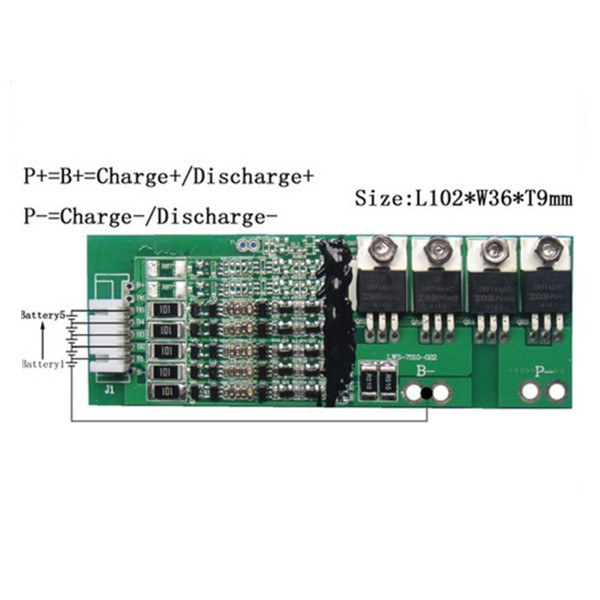
Detail Specifications for this 1.0mm board thickness 1oz green somdask smart home printed circuit
board PCB:
| Layers | 4 |
| Material | FR-4 |
| Board Thickness | 1.6mm |
| Copper Thickness | 1/1/1/1 oz |
| Surface Treatment | ENIG 2u" |
| Soldmask & Silkscreen | Green & White |
| Quality Standard | IPC Class 2, 100% E-testing |
| Certificates | TS16949, ISO9001, UL, RoHS |
What KAZ can do for you & your company
- PCB manufacturing
- components sourcing
- PCB Assembly: SMT/DIP services
In order to get a full quotation of the PCB/PCBA, pls provide below
information:
- Gerber, with detail specification of the PCB
- BOM List with excel fomart
- Photoes of the PCBA (if you have done this project before, if not,
just ignore this)
PCBA
design is the process of creating the layout and placement of components
for electronic circuits on a printed circuit board. Effective PCBA design is vital to the successful manufacture and operation of electronic
devices. The following are some key aspects of PCBA design:
Schematic Capture :
Define the functionality and connections of electronic circuits.
Choose appropriate components and packaging.
Ensures logical flow and adherence to design rules.
PCB Layout:
Define board dimensions, shape and layer structure.
Place components optimally for functionality, thermal management,
and manufacturability.
Route cables to connect components while taking into account signal
integrity, power distribution, and electromagnetic compatibility
(EMC).
Incorporate design-for-manufacturing (DFM) guidelines.
Component selection and placing:
Select components based on electrical, mechanical, and
environmental requirements.
Arrange components to minimize trace lengths, optimize signal paths
and ease assembly.
Consider component orientation, cooling, and access for testing or
rework.
Power Design:
Design an efficient power distribution network for different
voltage rails.
Implement decoupling capacitors, voltage regulators and other power
management circuitry.
Make sure to ground it properly and minimize noise/ripple.
Signal Integrity and EMC:
Control trace impedance, routing and termination of high-speed
digital signals.
Implement shielding, filtering, and other techniques to mitigate
electromagnetic interference (EMI).
Consider electrostatic discharge (ESD) protection.
Thermal management:
Identify heating components and provide adequate cooling solutions.
Incorporate thermal vias, heat sinks, and airflow considerations.
Testing and Manufacturability:
Incorporate test points, jumpers and other features to facilitate
in-circuit testing.
Follow DFM guidelines regarding solder mask, screen printing, and
other assembly related aspects.
PCBA design typically involves the use of specialized CAD (computer-aided
design) software, such as Altium Designer, Eagle, or KiCad, to
capture the schematic, lay out the PCB, and generate the necessary
manufacturing files.
PCBA design complexity varies depending on project requirements, component
density, signal speed, and other factors. Effective PCBA design requires a good understanding of electronic circuit principles,
manufacturing processes, and design best practices.
More detail photoes for this 4 layers ENIG 2u surface FR4 PCB with min 3/3 mil line width/space