Heavey Copper PCB printed circuit board PCB Assembly Service PCBA
Design PCB Assembly Service
Features
- Material: FR4 Tg180, 6-layer
- Minimum trace/space: 0.1mm
- Blind and buries via and via in pad
- Material: FR4, high Tg
- RoHS Directive-compliant
- Board thickness: 0.4-5.0 mm +/-10%
- Layer count: 1-22 layers
- Copper weight: 0.5-5oz
- Min finish hole side: 8 mils
- Laser drill: 4 mils
- Min trace width/space: 4/4 mils (production), 3/3 mils (sample run)
- Solder mask: green, blue, white, black, blue and yellow
- Legend: white, black and yellow
- Max board dimensions: 18*2 inches
- Finish type options: gold, silver, tin, hard gold, HASL, LF HASL
- Inspection standard: ipc-A-600H/IPC-6012B, class 2/3
- Electronic test: 100%
- Report: final inspection, E-test, solder ability test, micro
section
- Certifications: UL, SGS, RoHS Directive-compliant , ISO 9001:2008,
ISO/TS16949:2009
PCBA Technical capability
| SMT | Position accuracy:20 um |
| Components size:0.4×0.2mm(01005) —130×79mm,Flip-CHIP,QFP,BGA,POP |
| Max. component height::25mm |
| Max. PCB size:680×500mm |
| Min. PCB size:no limited |
| PCB thickness:0.3 to 6mm |
| PCB weight:3KG |
| Wave-Solder | Max. PCB width:450mm |
| Min. PCB width: no limited |
| Component height:Top 120mm/Bot 15mm |
| Sweat-Solder | Metal type :part, whole, inlay, sidestep |
| Metal material:Copper , Aluminum |
| Surface Finish:plating Au, plating sliver , plating Sn |
| Air bladder rate:less than20% |
| Press-fit | Press range:0-50KN |
| Max. PCB size:800X600mm |
| Testing | ICT,Probe flying,burn-in,function test,temperature cycling |
Following are the key steps of Heavy
Copper PCB Assembly Service:
Materials and Components:
High Copper Content PCB (2oz, 4oz or 6oz copper thickness)
Heavy Electronic Components (e.g. Power Transistors, High Power
Resistors, Heat Sinks)
High Temperature Solder (e.g. High Melting Point Lead-Free Solder)
High Quality Solder Paste
PCB Assembly Process:
PCB Preparation:
Clean PCB surface thoroughly to remove any contaminants.
Apply solder mask and silk screen as per component placement
requirements.
Drill and through holes for component leads and mounting.
Component Placement:
Carefully place components on PCB ensuring proper orientation and
alignment.
Secure component leads to PCB pads using high temperature solder
paste.
Reflow Soldering:
Place assembled PCB in reflow oven or use hot air rework station.
Heat PCB to appropriate reflow temperature (usually 230°C to 260°C)
to melt solder paste.
Ensure proper solder wetting and joint formation for all component
connections.
Inspection and Testing:
Visually inspect the PCB for any solder bridges, cold joints, or
missing components.
Perform electrical tests to verify the functionality of the
circuit, such as continuity, resistance, and voltage measurements.
Perform any necessary functional tests to ensure the circuit meets
design specifications.
Thermal Management:
Identify high-power components that require additional cooling.
Install heat sinks or other thermal management solutions as needed
to effectively dissipate heat.
Ensure proper thermal interface between components and heat sink.
Conformal Coating (Optional):
Apply conformal coatings, such as acrylic or polyurethane, to
protect the PCB and components from environmental factors such as
moisture, dust, and corrosion.
Final Assembly and Packaging:
Secure the PCB in a suitable housing or enclosure, if required.
Pack the assembled PCB for safe shipping and delivery.
Key Considerations for Heavy Copper PCB Assembly:
Ensure the PCB material and copper thickness are appropriate for
the power requirements of the application.
Select components with appropriate power ratings and heat
dissipation capabilities.
Use high-temperature solder and solder paste to withstand higher
operating temperatures.
Implement proper thermal management solutions to prevent components
from overheating.
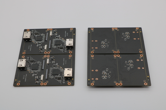
PCBA Pictures